The hardware
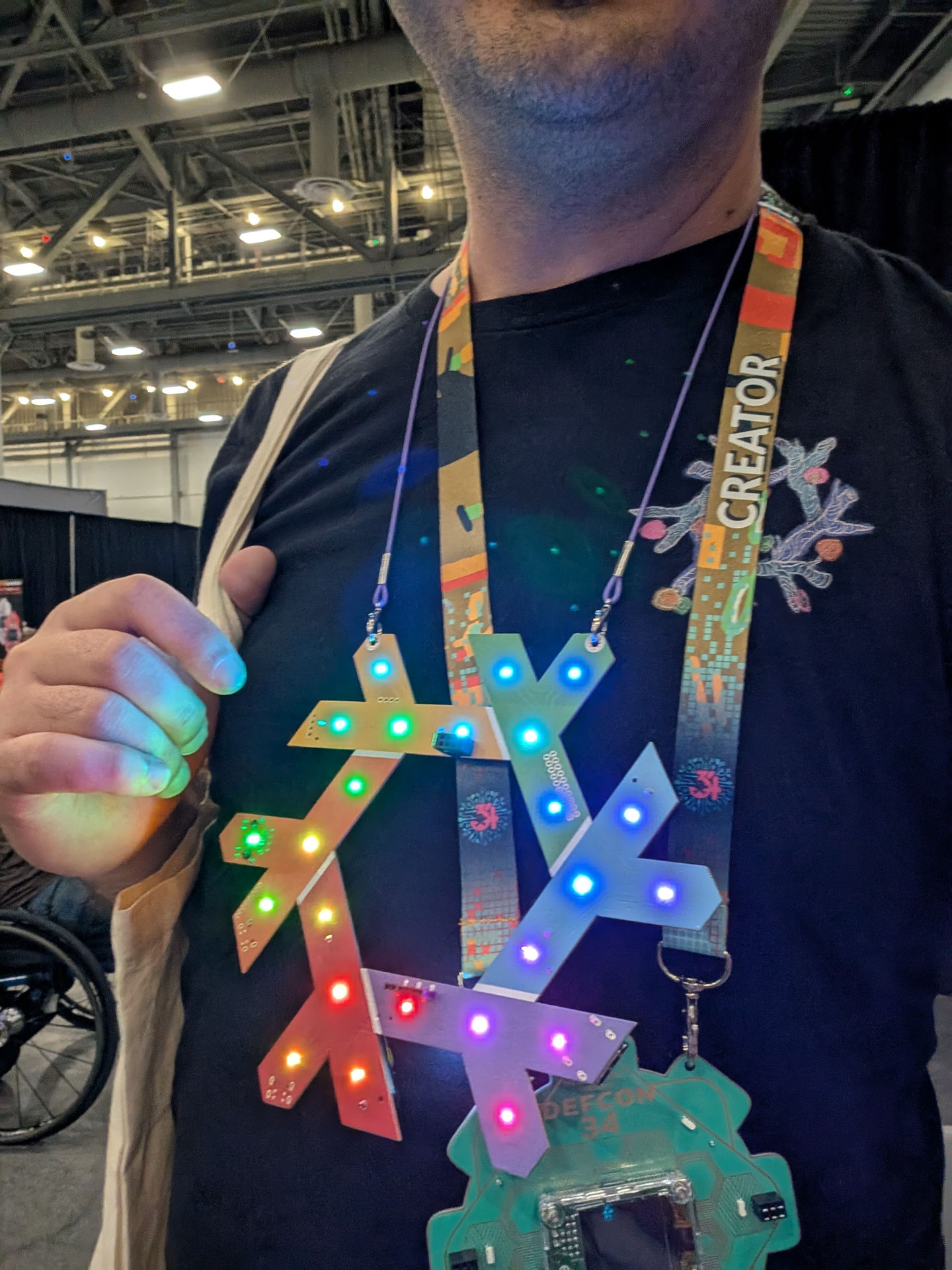
The reference designators (J6, S3 and so on) come from the KiCad
project, and everything here matches the v2.0 board
that was fabricated (commit 07f6efc; later commits only touch the silkscreen and the
README).
What the labels mean
| Silkscreen | Part | What it is |
|---|---|---|
| LUSTRATE | SW2 | The power switch for the batteries. Plugging in USB powers the badge without it. |
builtins.currentSystem | SW1 | The core switch: ARM, RISC-V, or AUTO (see Switching CPU cores) |
| BOOT | S1 | Picks the desktop profile at power-up; it’s also the mask ROM’s recovery strap |
| BUTTON | S3 | The general purpose button, which picks the video profile at power-up and drives the LEDs and screens afterwards. The software calls it USER. |
| RESET | S2 | Resets the module |
| DEBUG | J1 | USB-C to the on-board CH347, which gives you the serial console (115200 8N1) and JTAG, and powers the badge |
| USB | J9 | The module’s own USB-C port, a USB network adapter by default or a USB host in the desktop profile |
| ETH | J3 | 10/100 Ethernet, from the SoC’s built-in PHY |
| SD | J4 | The microSD slot |
| HDMI | HDMI1 | HDMI out, through the LT8912B MIPI-DSI bridge |
| SAO | SAO1 | The SAO connector (see below) |
| OLED | J7 | A 4-pin I2C header for an SSD1306 or SH1106 OLED |
| PWR | D5 (red) | Power-good from the 3.3 V regulator |
| ACT | D8 (green) | Activity on the CH347 |
| STAT | D3 (white) | A status LED driven by the SoC |
There are also a few headers without a label on the silkscreen: J6, the big 2x10 header; J5, the front header for the Sharp Memory Display; J8, a second OLED header wired the same way as J7; and J2, a small 2 mm header on the JTAG and console lines.
The silkscreen has a few power notes too. HDMI only gets its 5 V when the badge is on USB power, so it won’t work on batteries alone. USB host mode on the USB port needs power coming in through the DEBUG port. The HDMI link has the details of the HDMI output.
The 2x10 header (J6)
J6 is a 2.54 mm 2x10 header on the back of the badge, and it’s the main place to hang your own hardware off the badge. Odd pins are on one row and even pins on the other:
| Pin | Signal | Pin | Signal | |
|---|---|---|---|---|
| 1 | VSEL | 2 | +3.3 V | |
| 3 | LCD_RST (also BUTTON) | 4 | SPI3_CS | |
| 5 | LCD_PWR_CT | 6 | SPI3_SDI | |
| 7 | LCD_PWM | 8 | SPI3_SDO | |
| 9 | PWM0_BUCK | 10 | SPI3_SCK | |
| 11 | SAO_GPIO2 | 12 | I2C1 SCL | |
| 13 | +1.8 V | 14 | I2C1 SDA | |
| 15 | +1.8 V | 16 | GND | |
| 17 | ADC3 | 18 | GND | |
| 19 | GND | 20 | GND |
A few things to know about these pins:
- VSEL is whatever is powering the badge at the moment, so it’s about 5 V on USB power and the battery pack’s voltage on batteries. The +1.8 V pins come from the same regulator as the HDMI bridge, so don’t load them much while HDMI is running.
- SPI3 is the same bus that drives the LED ring. The ring gets SPI3_SDO through an AND
gate (U10) with SPI3_CS, so it only listens while CS is high, and every time CS goes
low for another device the ring sees it as the end of a frame. A device on SPI3 has to
share the bus with
nix-badge-bling, which owns/dev/spidev3.0. - I2C1 is the bus the OLED headers use (
/dev/i2c-1), on the module’s side of the SAO’s bus switch, so anything you put here shows up next to the OLED. - LCD_RST is the module’s LCD_RST pin, which is
PWR_GPIO2in the SoC’s always-on RTC domain. BUTTON is wired to it through a 100 Ω resistor, with a 10 kΩ pull-up to 1.8 V, so it reads low while BUTTON is pressed. It’s a 1.8 V-only pad, so never drive it above 1.8 V. - LCD_PWR_CT and LCD_PWM are the module’s pins 37 and 38, and are otherwise unused on the badge.
- PWM0_BUCK and SAO_GPIO2 are GPIO lines 0 and 19 on the SoC’s second GPIO controller,
named
pwm0-buckandsao-gpio2in the device tree. - ADC3 goes straight to a SARADC input with no divider, and Linux reads it as IIO
channel 2 (
in_voltage2_rawtimesin_voltage_scalegives millivolts). The other two channels measure VSEL and the battery through dividers.
The SAO connector
The SAO connector follows the newest SAO spec, v1.69bis (also called SAOv2, see badge.life). It’s mounted upside down, the same way as on this year’s official DEF CON badge, so an add-on hangs the other way up from what you’d expect. Check where pin 1 is before you plug one in.
| Pin | Signal |
|---|---|
| 1 | 3.3 V, switched and current-limited (U13) |
| 2 | GND |
| 3 | I2C1 SDA |
| 4 | I2C1 SCL |
| 5 | GPIO1: the LED ring’s data out |
| 6 | GPIO2: sao-gpio2 |
The connector’s power and signals go through a load switch (U13) and a bus switch (U12),
which BadgeOS turns on at boot. GPIO1 is the end of the LED ring’s WS2812 chain,
buffered, so an add-on with its own WS2812s can sit at the end of the chain. Raise the LED
count in badge.bling to drive them.
The other headers
J5, the front header for a Sharp Memory
Display, is a 1x6 2.54 mm header on SPI3. The
display shows up as the text console on tty1.
| Pin | Signal |
|---|---|
| 1 | VSEL |
| 2 | Not connected |
| 3 | GND |
| 4 | SPI3_SCK |
| 5 | SPI3_SDO |
| 6 | CS, which is SPI3_CS inverted (Q7) because the display’s chip select is active high |
J7 (labelled OLED) and J8 are 1x4 2.54 mm headers for an I2C OLED, in the usual pin order for the cheap SSD1306 modules:
| Pin | Signal |
|---|---|
| 1 | GND |
| 2 | VSEL |
| 3 | I2C1 SCL |
| 4 | I2C1 SDA |
J2 is a 1x8 2 mm header on the 3.3 V lines between the CH347 and the module. The JTAG lines have 33 Ω resistors between the CH347 and the module, and J2 sits on the CH347’s side of them.
| Pin | Signal |
|---|---|
| 1 | GND |
| 2 | TCK |
| 3 | TDO |
| 4 | TDI |
| 5 | TMS |
| 6 | TRST |
| 7 | UART0 TX (the console) |
| 8 | UART0 RX |
Power and the LED ring
The badge runs on three AA cells in series (BT1 to BT3) or on USB, with USB taking priority when it’s plugged in. A TPS63020 buck-boost makes the 3.3 V rail from that, and an RT9080 makes 1.8 V for the HDMI bridge. The RTC and the core-select latch stay powered from a tap after the first two cells (or from 3.3 V when that’s up, which is what “VRTC 2xAA/3v3” on the silkscreen means), with a supercapacitor to keep the RTC alive while you swap batteries.
The 24 WS2812 LEDs in the ring (LED1 to LED24) run from VSEL rather than the 3.3 V rail, on purpose. When the batteries get low, the ring turns into red glitch art, which we thought was more interesting than having it just dim out.